Optimized Surface Mount Technology (SMT) Production Line
Increased capacity and efficiency by integrating prototype Printed Circuit Boards (PCBs), streamlining existing workflows, and fine-tuning equipment calibration, resulting in improved quality, on-time delivery, and scalability for future demands.
Equipment & Resources Upgrade
- Increase Feeder Capacity - Qty 50 for 2 parts numbers that are always loaded
- Automatic Optical Inspection (AOI) Machine upgrade - New vs used price comparison
- Additional Head (SMT) - Increase throughput with 7 spindle Flex Jet vs 4 spindle head
- Preventive Maintenance - Nozzle calibration
- Approve Resources - Dedicate Operators to specific stations
Stencil Printing Process
- Squeegee release performance - Need consistent well controlled paste thickness
- Solder Paste Dispensing - Desirable in moderate tack
Pick & Place Machine Optimization
- Improve Rate - Data collection analysis via time studies
Reflow Profile Development
- Improve Heating & Cooling Rates - Less stress and stronger joints
Reflow Profile Process Development

Solder Joint Defects Detected During Reflow with Solutions
Cold Solder - Dull, grainy or uneven appearance. Component does not properly bond to the component lead or PCB pad. Poor electrical conductivity. Fragile, making it prone to break at stress.
Tomb-stoning - One end of a chip component (eg. resistor, capacitor), lifts of the PCB pad during reflow soldering process. This causes component to stand up, resembling a tombstone.
Non-wetting - Area where solder may be in contact but does not form metallurgical bonding with the base metal, such as unvetted spot within solder joint.
De-wetting - Appearance of water on a greasy surface. It is wetted initially but retracts over time causing the solder to collect into discrete globules and ridges.
Issue:
- Insufficient Heat: Not reaching peak temp to fully melt and bond
- Rapid Heating / Cooling: Can prevent proper solder flow and joint formation
- Uneven Heating: Poor thermal distribution or improper calibrated reflow profile
- Oxidized Surface: Prevents proper wetting
- Excessive or Insufficient Solder Paste: Results in incomplete bonding
- Design Issues: Poorly designed thermal relief pads impede heat transfer
Solutions:
- Optimize Reflow Profile - Match solder paste specs, and follow 4 key phases
- Preheat Zone: Gradually preheat the board to avoid thermal shock & ensure proper flux activation. Typical ramp up is 1-3 °C / second.
- Soak Zone: Allow for sufficient soak times, typically (60-120 sec). Maintain steady temperature to distribute heat, activate flux and remove oxides.
- Reflow Zone: Heat above solder's paste melting point for adequate wetting & bonding. Peak temperatures 210 - 250 °C. Lead free tends to be on high end. Time Above Liquids (TAL) is 30 - 90 sec per solder spec. Avoid under heating to eliminate cold solder joints. Overheating can damage components.
- Cooling Zone: Controlled cooling to solidify joints without including thermal stress. Avoid rapid cooling which can induce stresses and voids.
Surface Mount Technology (SMT) Typical Defects

Tomb-Stoning
Tomb-Stoning
Tomb-Stoning
Tombstoning is typically caused by imbalances in solder paste application, such as uneven volume or misalignment, or by uneven heating and cooling rates during reflow soldering. When one end of component heats faster than the other, surface tension pulls the component upright, resulting in open circuit. This highlights importance of precise solder paste application and controlled thermal profiles.
Cold Solder
Tomb-Stoning
Tomb-Stoning
Solder connections are poorly bonded if light easily passes through the junction, indicating gaps or weak adhesion. Characterized by a rough or dull appearance, typically result from insufficient heat during soldering. In electronic applications, PCBs heat up during operation, and these thermal cycles can worsen weak or poorly formed solder joints, increasing the risk of failure over time.
Non-Wetting
Tomb-Stoning
Non-Wetting
Wetting in soldering is the effect where molten solder covers the soldered surface evenly without gaps, forming an inter metallic phase. The wetting angle between the solder and the soldered surface is less than 90°. The molten solder spreads across the surface, creating a uniform layer. Non-wetting, the opposite of wetting, is the inability of molten solder to form a metallic bond with the base.
Surface Mount Technology (SMT) Process
Reflow Soldering Process
- Reflow soldering is a common method for attaching surface-mount components to printed circuit boards (PCBs). The process involves pre-heating the components, PCB, and solder paste, followed by melting solder to form acceptable solder joints, while carefully avoiding damage from overheating.
- The key aspect that lead to an effective reflow soldering process are as follows:
- Proper Machine Selection
- Acceptable reflow profile
- PCB / component footprint design
- Accurately printed PCB using well designed stencil
- Repeatable placement of surface mount components
- Good quality PCB, components and solder paste

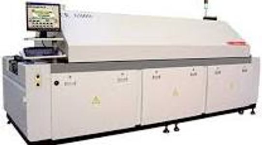
Proper Machine Selection
- The type reflow soldering machine depends on the required line speed and design/material of the PCB assemblies to be processed. The selected oven needs to be of a suitable size to handle the production rate of the pick and place equipment.
- Line speed (minimum) = Boards per min x Length per board / Load Factor (space between boards)
- To select the correct size reflow, process speed must be greater than minimum calculated line speed.
- Process speed = Oven chamber heated length / Process dwell time. NOTE calculation is for heated length.
- Design of PCB assembly will influence the machine selection and what options are added to the following specification:
- Conveyor type
- Closed loop control for speed of convection fans
- Automatic control of conveyor and centre-board support widths
Acceptable Reflow Profile
- Within a typical reflow soldering profile there are four stages - Preheat, soak, reflow and cooling. Intention is to transfer enough heat into the assembly to melt the solder and form solder joints without causing damage to components.
- Each assembly needs to be considered separately as there are different aspects that affect reflow oven programming:
- Type of solder paste
- PCB material / thickness
- Number of layers
- Amount of copper within PCB
- Number of surface mount components
Reflow Profile 4 Stages
- Preheat - PCB and solder are all heated to a specified soak or dwell temperature making sure not to heat too quickly. Usually no more than 2°C/second. Fast rates can cause cracks and solder splatter.
- Soak - Purpose is to ensure all components are up to the required temperature before entering the reflow stage. Typical soak last between 60 and 120 seconds depending on the mass differential of the assembly. The more efficient the heat transfer during the soak phase the less time is needed.
- Reflow - The temperature within the reflow oven is increased above the melting point of the solder paste causing it to form a liquid. The time the solder is held above its melting point (time above liquidus) to ensure correct wetting occurs between components and PCB. This is time is typically 30 to 60 seconds. Important to control peak temperature.
- Cooling - Stage during which the assembly is cooled making sure its not done too rapidly. Usual recommended rate 3°C/second